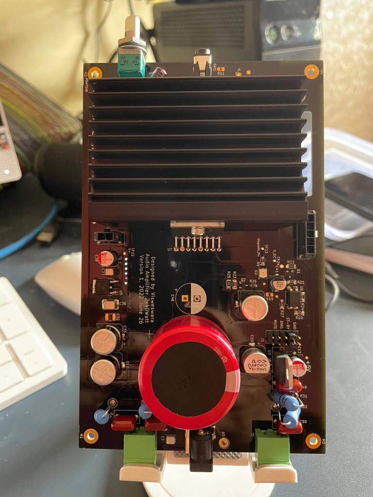
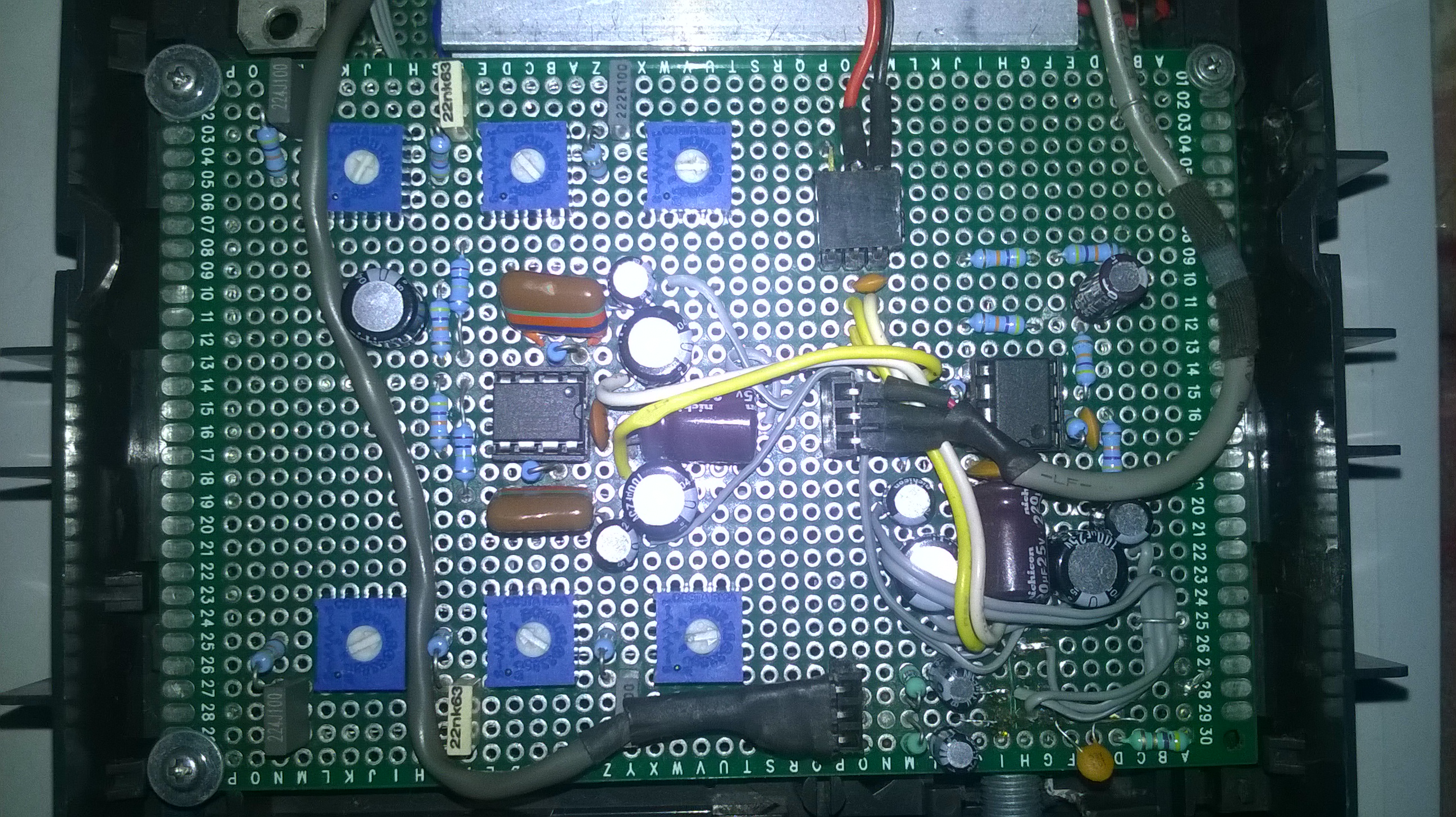
Audio Amplifier, STEREO 40+40 watt Amplifier.
My recent project did in june 2022, wanted to share some pictures of it.
Final output.


Audio Amplifier, STEREO 40+40 watt Amplifier.
My recent project did in june 2022, wanted to share some pictures of it.
Final output.
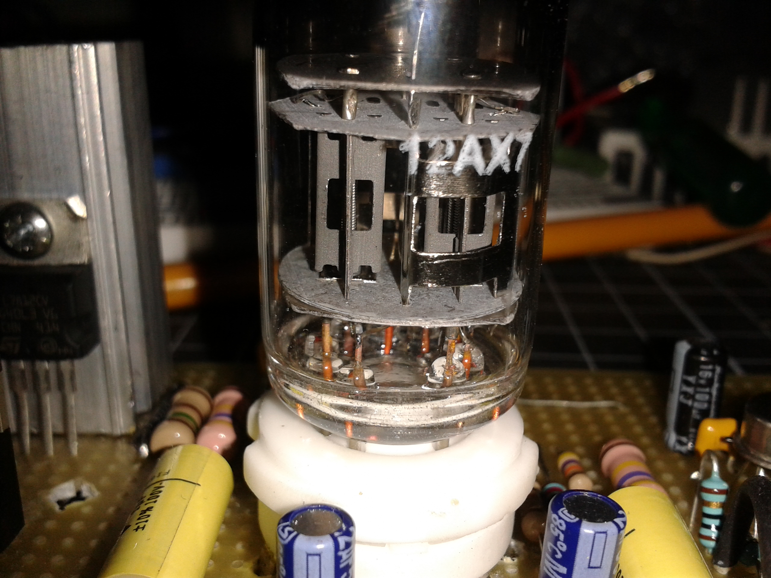
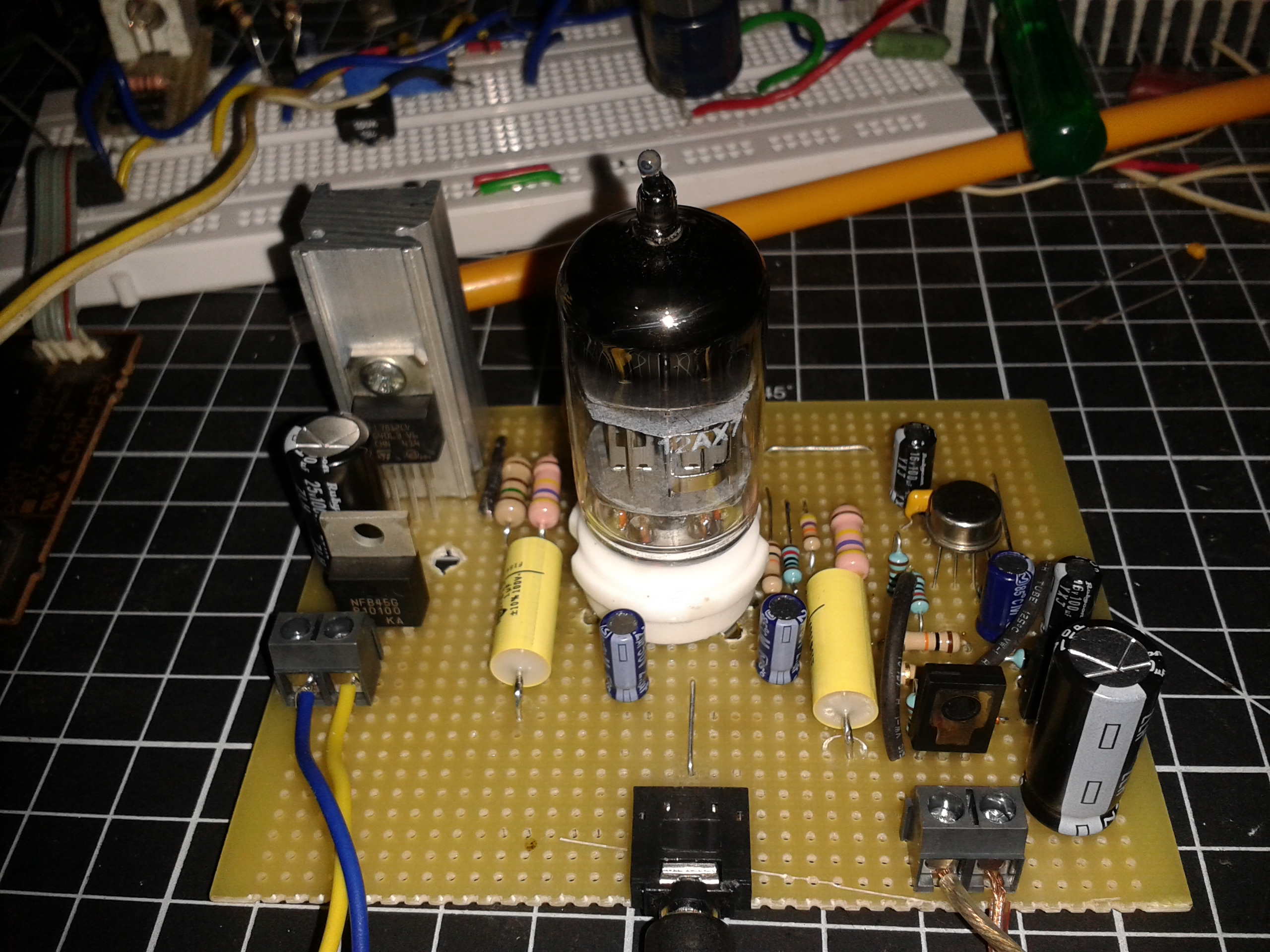
I always wanted to build vacuum tube or valve amplifier. finally I made one hybrid amp. just combined both valve and solid state. For the preamp section I have used 12ax7(dual triode) and for the solid state I built opamp based power amp configured in unity gain..
This is the low power version and I’m sure I am going to build medium power amp delivers atleast 5-10watts to the speaker and no solid state 😀
Here is the picture of my construction:
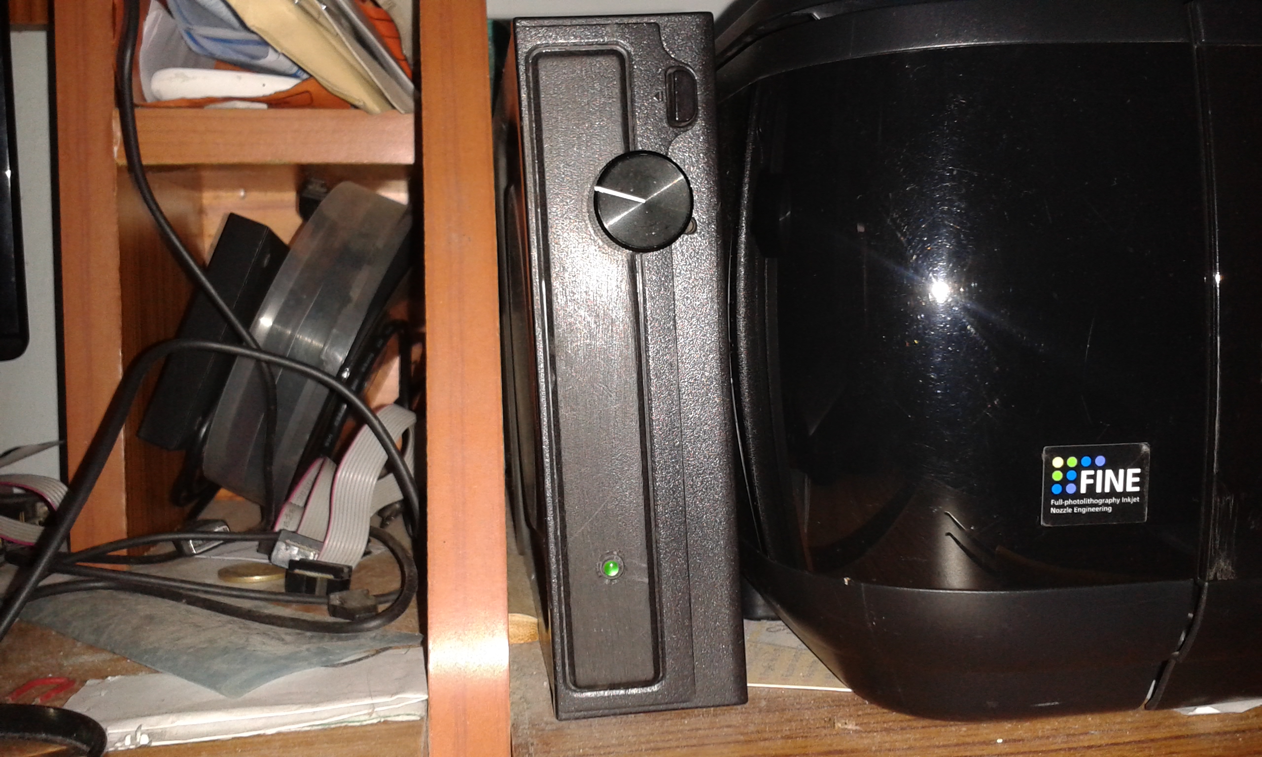
Audio exciter:
Exciter is also known as bodyshaker, Audio Exciter is just basically a loud speaker without a membrane, and it consists of voice coil , oscillating mass and mounting ring/plate. If the audio/music signal is applied to the contact pins of the voice coil, the oscillating mass starts shaking with the frequency of the applied music, the oscillation is transmitted to the mounting ring and from there on to the surface the exciter sticks to, thus the excited surface emits the music signal.

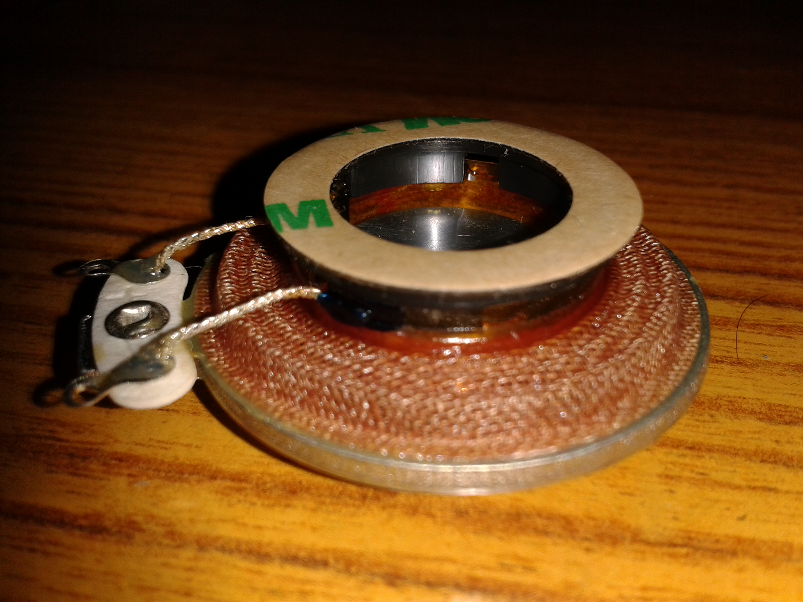
For testing the audio exciter I did built a small opamp based amplifier which delivers 2Watts rms at 6ohms impedance 
This amplifier circuit is nothing new. and you can find a better one here (discrete transistor amp)
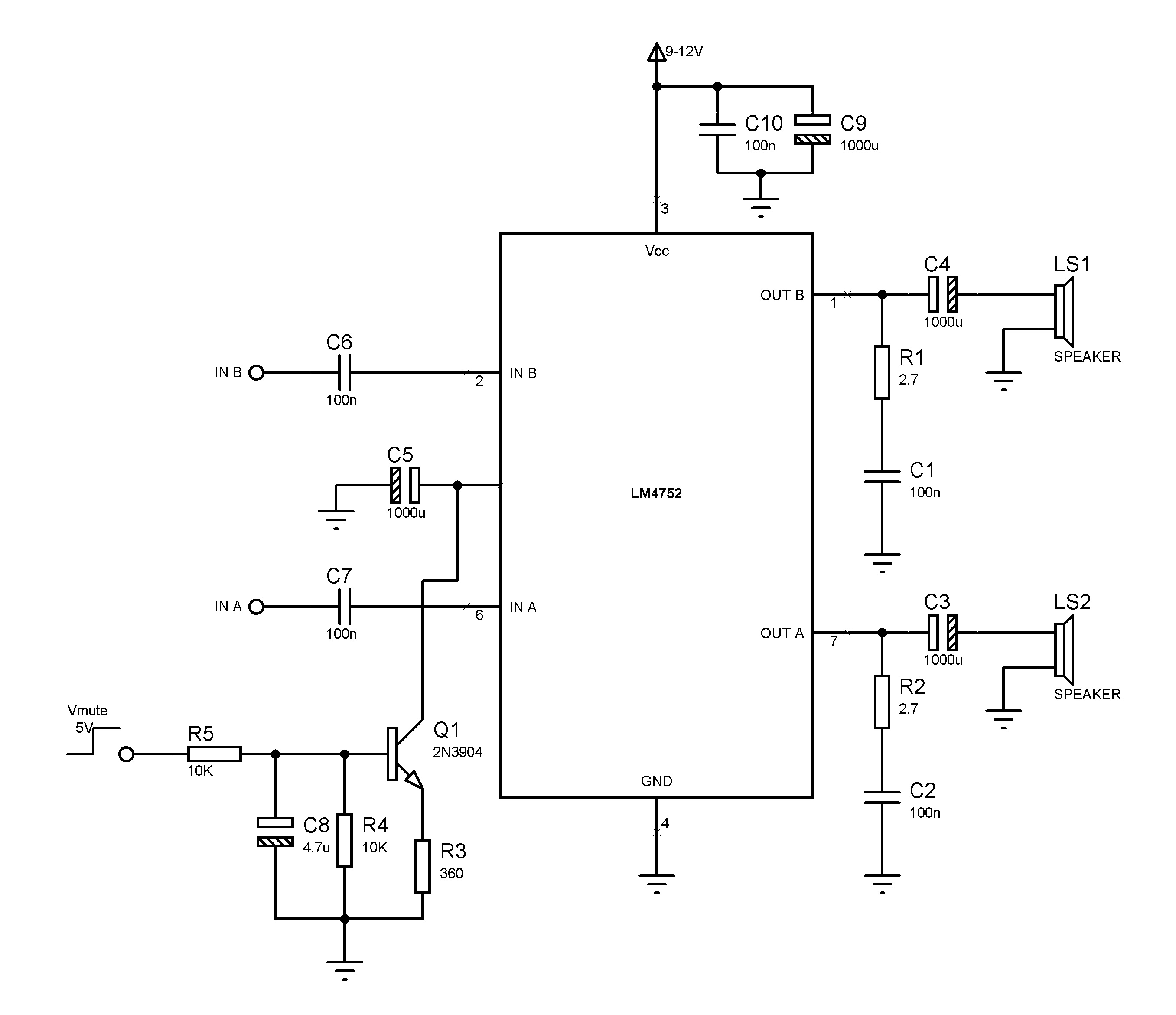
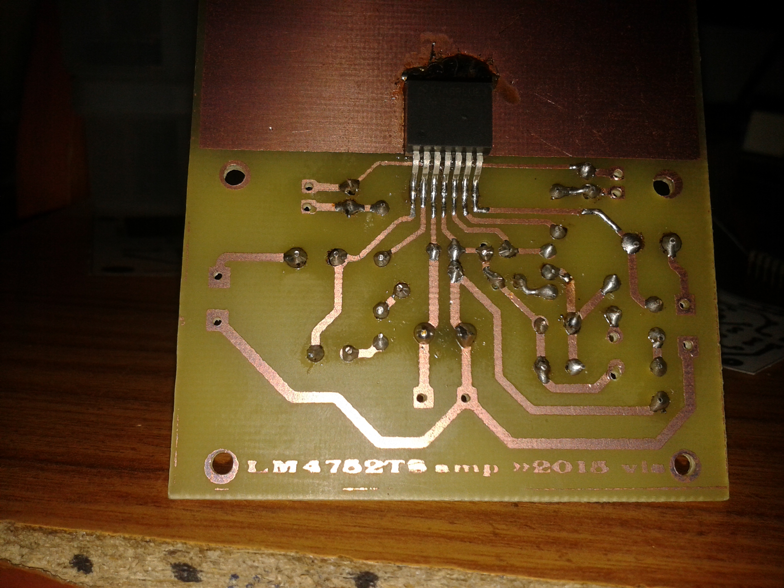
LM4752 is a stereo audio amplifier capable of delivering 11watt per channel of continuous average output power to a 4Ω load, or 7W per channel into 8Ω, using a single supply at 10% THD+N. A simple mute function can be implemented with the addition of a few external components.

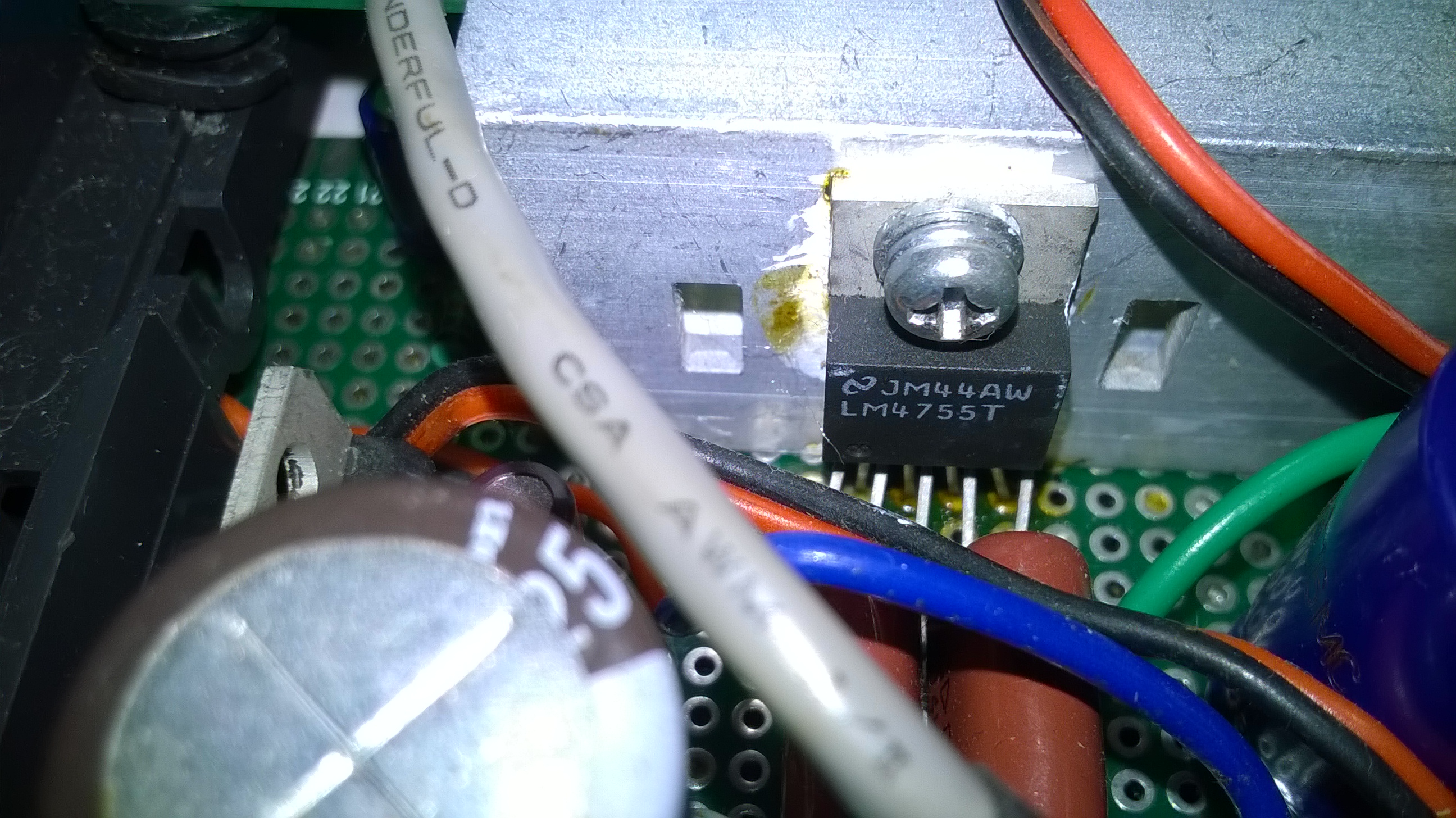
I built this amplifier for my iPod, amp circuit based on LM4755 chip, stereo audio amp capable of delivering 11watt per channel of continues average power output to a 4Ω using a supply of 24V at 10% THD. It is designed for single supply operation.
Features:
Construction- DIY LM4755 amp
This amp, primarly used on my desk. So it needs to look good, for the enclosure i used old dead CD-ROM case.
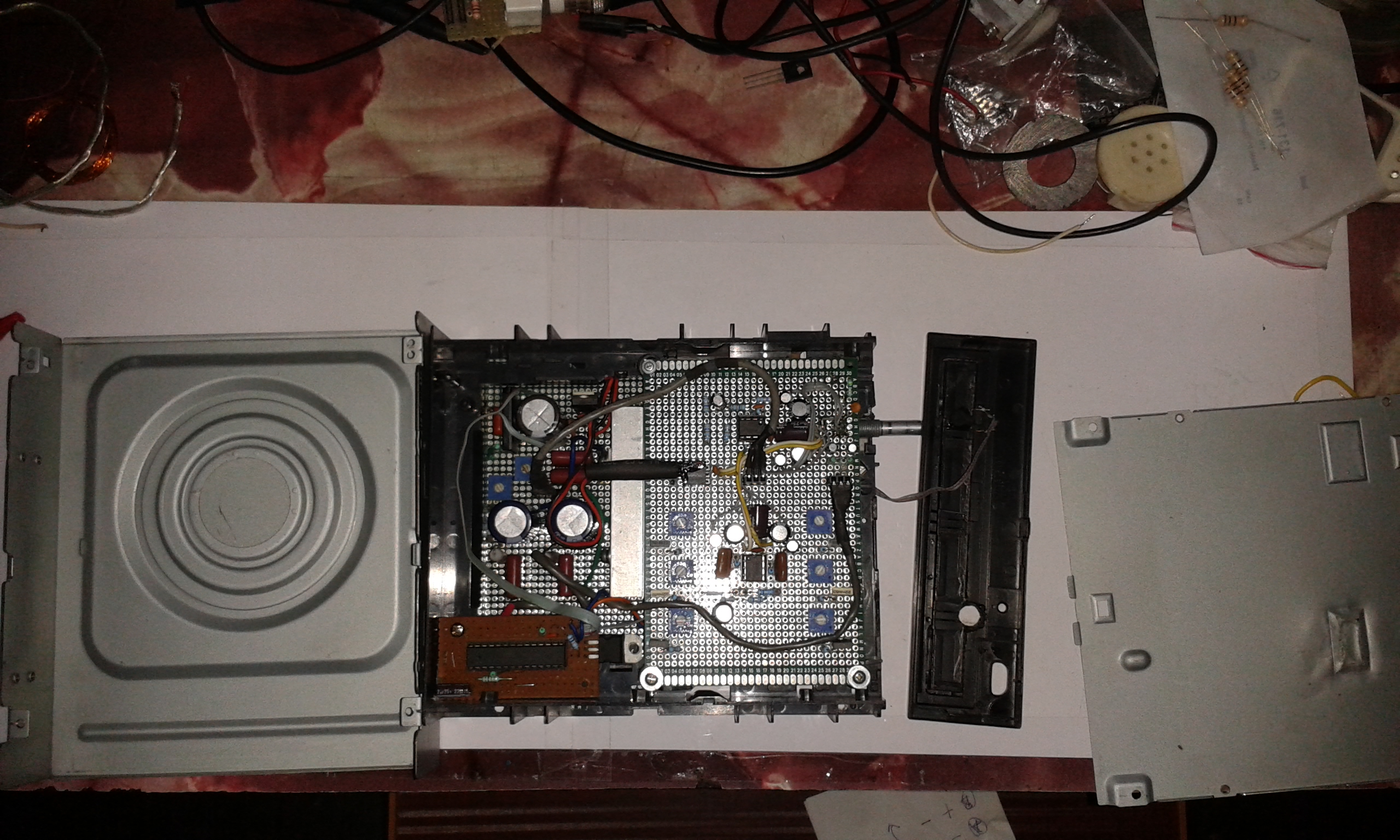
for tone control and preamplifier I used OPA2134 (dual opamp) chip.
preamp is 1.5dB gain that works with single power supply. and the tone control to boost or reduce the particular audio frequencies, simple RC filter circuit + preset/VR to control the Signal level of particular freq.
Pictures of my construction:


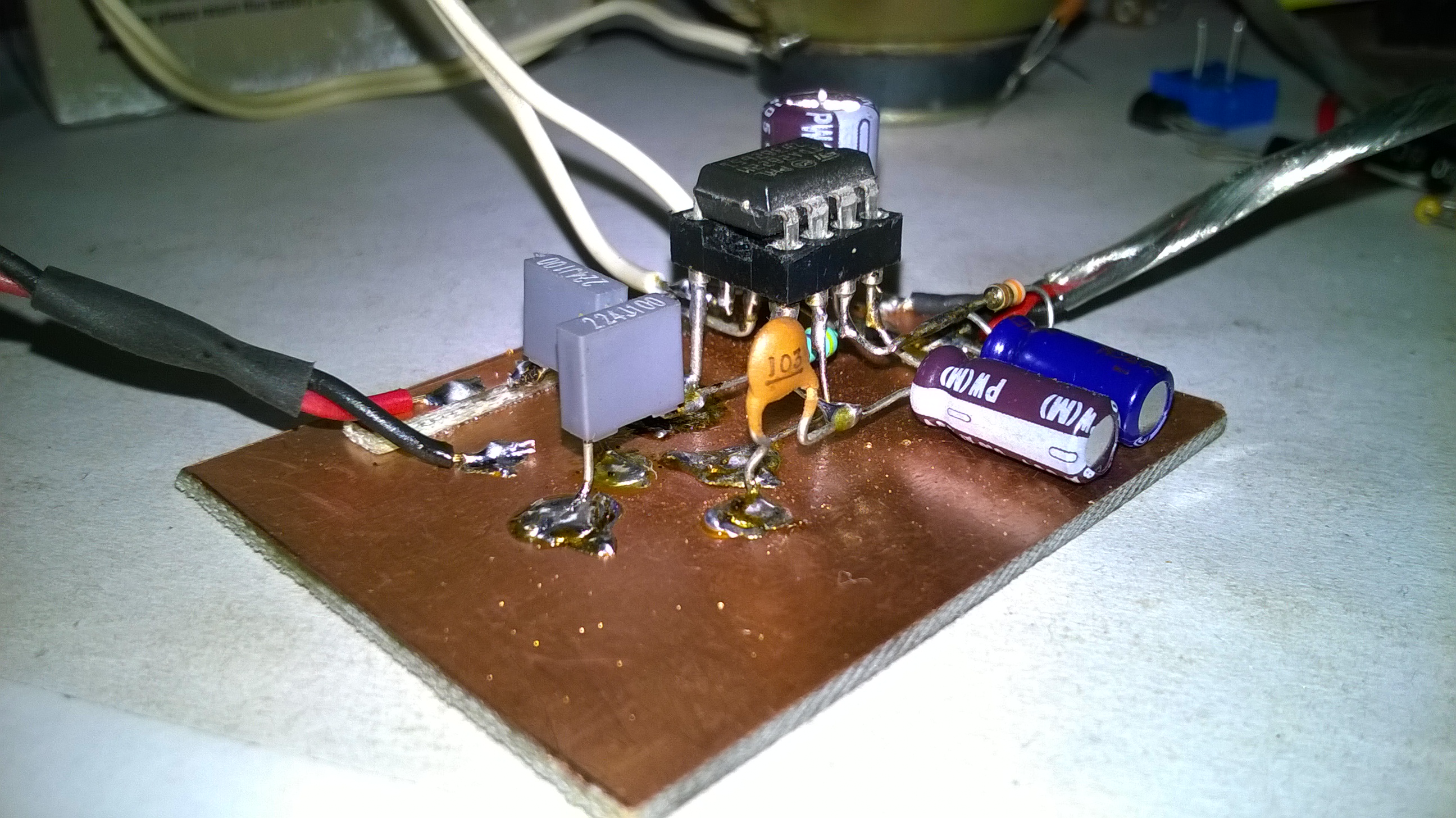
This is a part of my RF transceiver project, no parts for building tranceiver yet , so i have started with the audio amp circuit, amplifier circuit is based on TDA2822M chip which is configured in bridge mode and I used a single sided Copper plated board for Manhattan construction. 😛
circuit:
(nothing new it is from the datasheet)
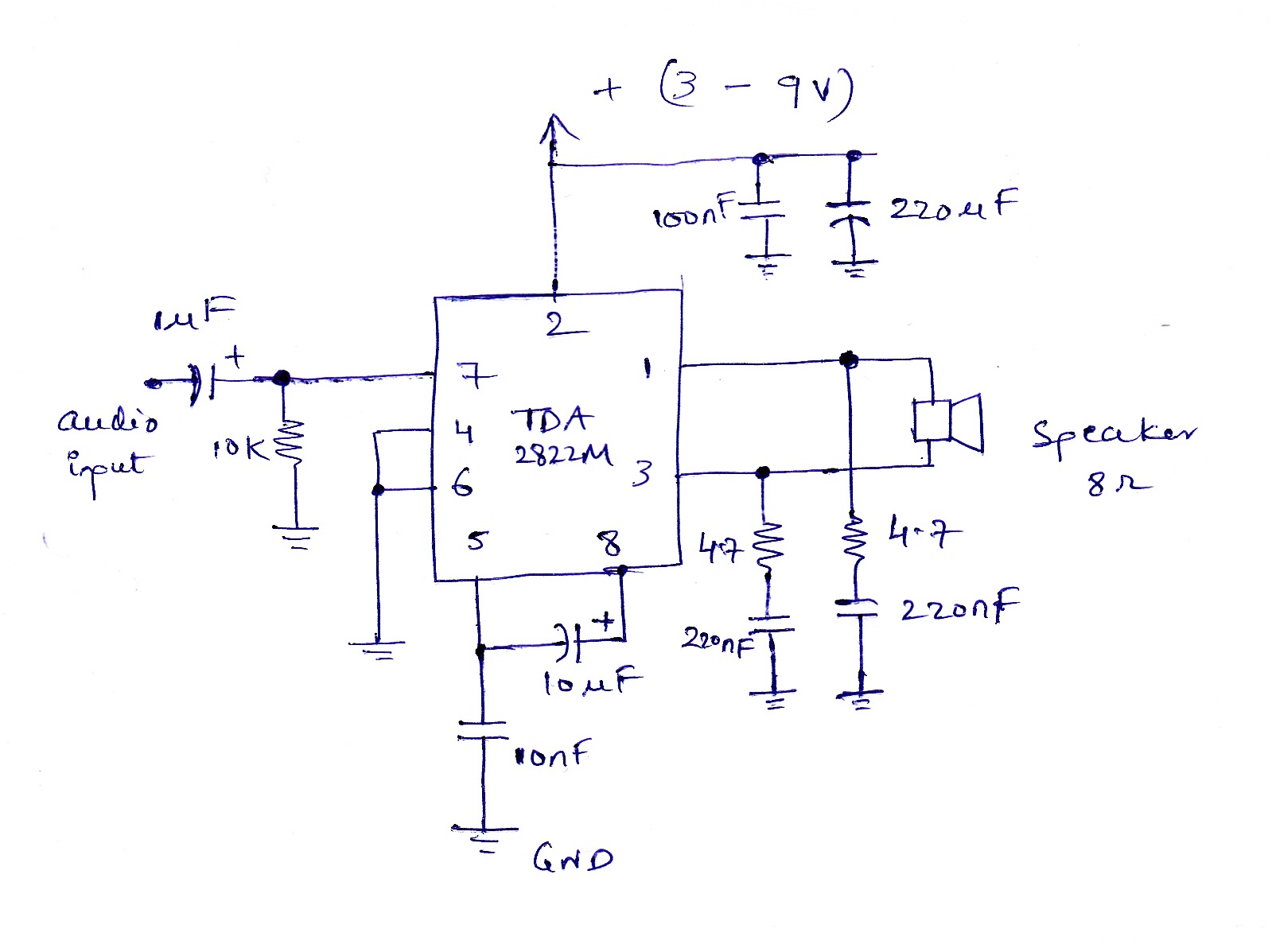
my construction
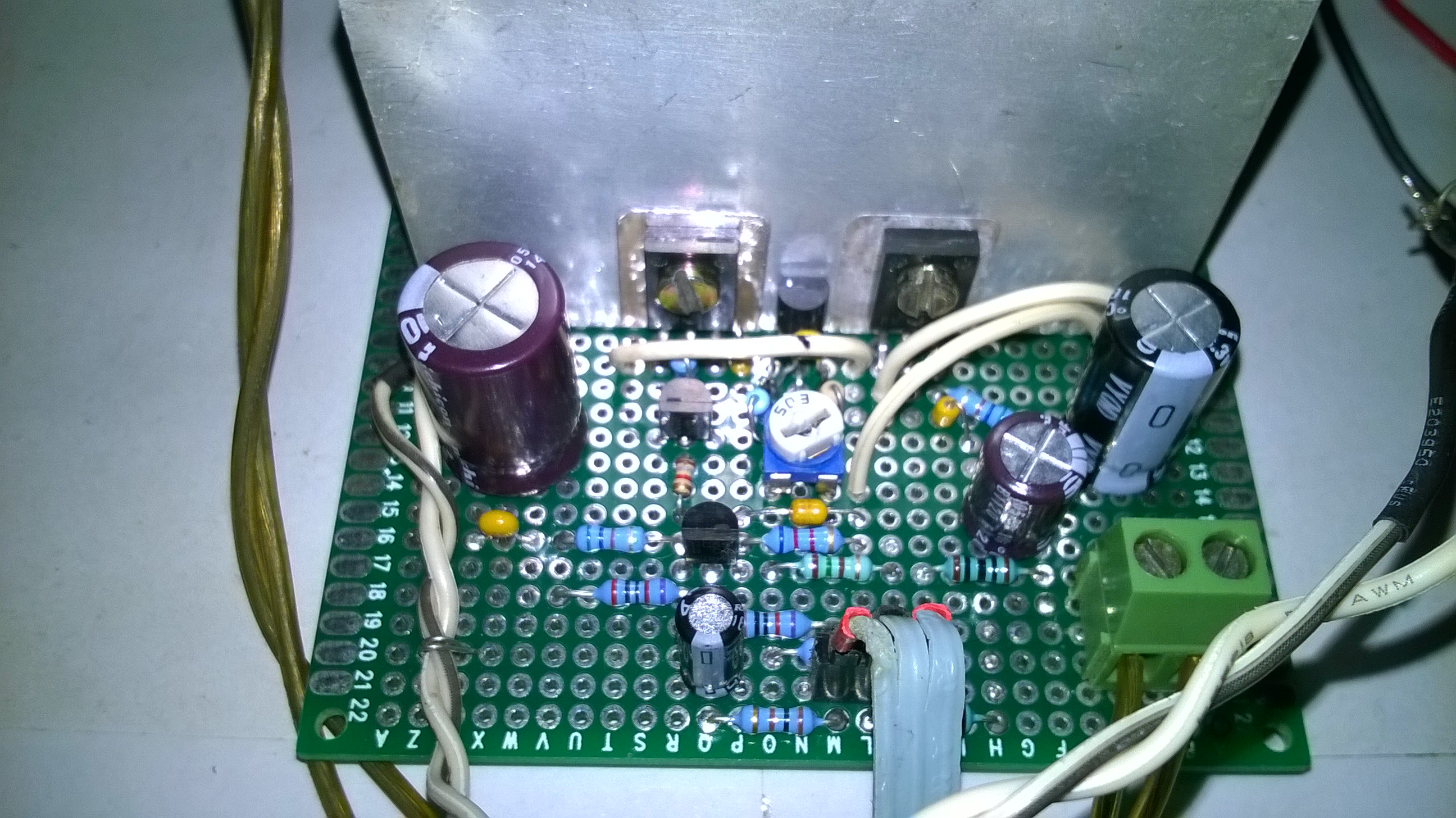
This is the small audio amplifier circuit, with decent power output of 3watts RMS into 4ohms load.
as you can see the pictures of my construction:


circuit diagram:
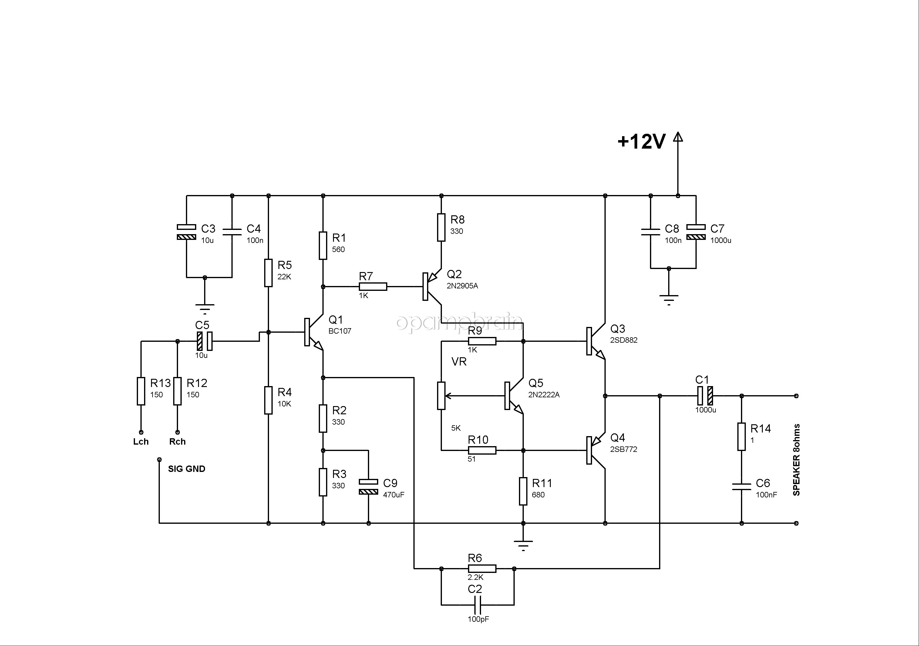
R4,R5 resistors forms voltage divider and biases the transistor Q1. the voltage across the R4 is (Vin*R4)/(R4+R5) 3.75Volts
R1 560 ohms set the collector current Ic of Q1 = (Vin-Vc)/560. Vc = 9.4volts measured with respect to GND so Ic = (12-9.4)/560 = 4.642mA
R2,R3 are the emitter resistors connected to Q1, since the Q1 is the input transistor of the amplifier circuit, so small ac signal appears across the emitter resistors, therefore low impedance path must be created to bypass the ac signal using capacitor C9 the value of c9 can be calculated by taking the two considerations into picture,
one is audio amplifier must cover the frequency range from 20Hz-20KHz and the other is the reactance of the capacitor should be 1/10 of the emitter resistance or less than the emitter resistance therefore Xc = 1/(2πfC) the c = 1/(2πfXc) , from this equation the capacitance is max at the lower frequency(20Hz) and Xc must be 1/10 of the emitter resistance
c = 1/(2 π×20×330/10) = 120.57uF = 120uF (which is standard) but rare 150uF is also standard also rare, I used 470uF.
Q2 , 2N2905A of motorola is the driver transistor(class A), this transistor is little old, you can use bd140 or 2N3906 instead, R7 is the base resistor and R7 is the collector resistor Q2 to keep the transistor in active region.(not a big gain at this stage)
R9,R10, VR 5K pot and Q5 , 2N2222A (can be 2N3904) forms the Vbe multiplier circuit to eliminate the cross over distortion, adjust VR to 1.7K up in series to the 1K(R9) s0 it forms (1.7K+1K). R11 and Vbe multiplier circuit controls the quiescent current to have thermal control over output the Q5 must be mounted to the main heatsink. this Vbe multiplier is a biasing diode but adjustable voltage drop.
Q3(CL100),Q4(CK100) are the output transistors. can also be replaced with famous bd139 and bd140. or 2sd882 and 2sb772
C1 is the output capacitor which is 1000uF, if you want to have good low frequency response , 3300uF is good.
R6, 2.2k (feedback resistor) in parallel with C2 1nF ceramic capacitor, creates a pole frequency of about 1/(2πRC) = 72.343KHz , feedback system keeps the amplifier linear and stable operation.
R14,C6 is to remove the high frequency noise..
C3,C4,C7,C8 are decoupling capacitors to remove high frequency, mid frequency and low frequency noise in the power supply lines
C5 is the input capacitor C5 and R4 together forms a high pass filter cutoff-frequency is 1/(2π×10uF×10K) = 1.59Hz.
R13,R12 (150 ohms) combines both the channels this resistors must be greater than 40 ohms, or else , effects the source device (ipod or music player etc…..)
here are the oscilloscope waveforms of neat 100KHz, square, ramp and sine wave ( R_load 7.5ohms )


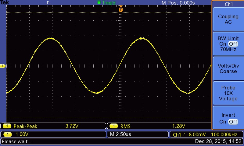
this amp sounds really good, from the scope results i did calculated THD, it is 2.5% at 3watts RMS output. frequency response is flat from 30Hz to 100KHz 😀