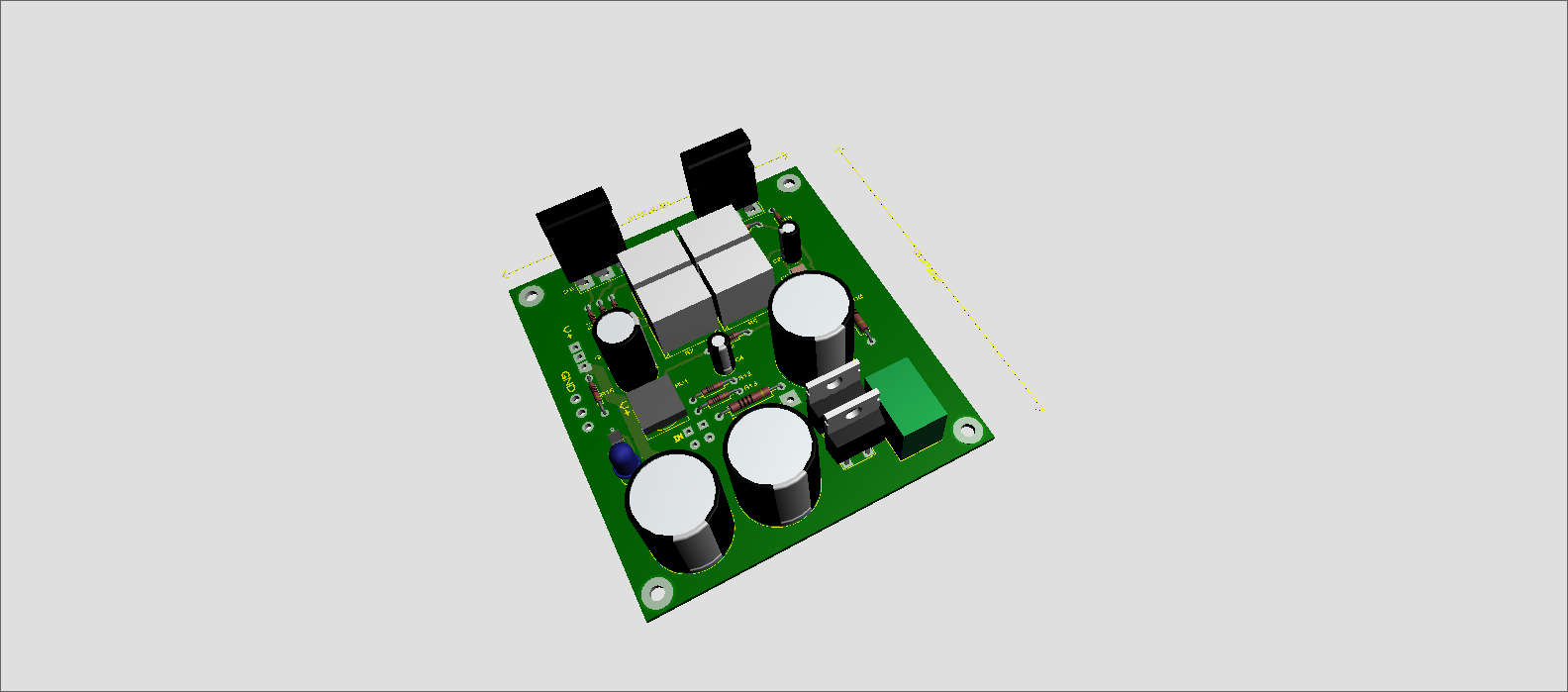
This circuit is built with TI sound plus op-amp OPA2134 and THD of the amplifier is less than 0.3% at 12watts RMS into 4ohms driver, very low noise we can achieve using this circuit and this circuit is powered by a single power supply which is very commonly available, Circuit built with dual op-amp(OPA2134) which is U1.

U1B is configured as Vref the output of this op-amp is exactly mid voltage of 20V as 20V/2 is 10V of supply to ensure to have a symmetrical and dynamic range of both input and output signals and it is configured by R8, R9 resistors and C1 buffer capacitor, value of C1 can be calculated as C1 = 1/(2π×fc×47000/2) where fc cutoff frequency should be <= 1/10th of input frequency(fin) signal, consider fin = 10Hz; fc=1Hz so C1= 1/(2π×1×23500) = 6.77µF, 6.8µF is rarely available, if available we can use, the commonly available value is 10uF, and the output of this opamp U1B is fed to U1A non-inverting terminal. C4 is the input capacitor to allow input signal, R11 is the gain setting input resistor and R12 serves as feedback resistor so the gain of the amplifier is calculated as 20log(82k/4.7K) = 24.83dB
The following is the scope screenshot1, probing both input and output signals of the amplifier.
 sine wave in blue is the input signal(740mV) and yellow the output (14.2V) inverted output
Gain = 20log(14.2/0.740) = 25.66dB which is almost equal to the calculated value of gain with resistors.
Input capacitor C4 value can be calculated = 1/(2π×fin×R11) = 1/(2π×10×4700) = 3.386µF The next higher value is 4.7µF.
C2 and C3 connected across op-amp power pins U1C are electrolytic and ceramic combinations to reduce low frequency and high frequency noise in the power supply lines and must be placed close to the op-amp power pins. Main filter capacitors are C5 and C6 to reduce noise in the supply lines; the ESR(Equivalent Series Resistance) of these capacitors must be low, for better noise reduction. R4 protects the op-amp output pin by not over driving the current it is less than 6mA and drives the Q2 transistor of Voltage amplification stage.
R13 is the current source,R1 , RV1 and Q4 forms Vbe multiplier also called as adjustable diode and its purpose to reduce the cross-over distortion by providing the bias voltage for the Voltage Amplification Stage (VAS)formed by complementary transistors Q1, Q2 and drop across R3 , the voltage Vce of Q4 is Vadj, this can be adjusted by varying RV1 setting it to 472Ω.
Voltage acrossR1 = 1.3mA×1000 = 1.3V and the
Voltage drop across RV1 = 1.3mA×472=0.6136
Vadj can be calculated by VRV1×((R1+RV1)/RV1)) = 0.6136×((1000+472)/472)= 1.9136volts
The Vbe multiplier also acts as thermal feedback unit as Q3 and Q5 get hot during operation, Q4 senses the heat and controls the collector current by reducing base of Q1 and Q2. Q4 must be placed/slabbed to the heatsink or closely to the Q3 and Q5, Vbe multiplier plays a critical role in an amplifier to make the circuit thermally stable. Emitter current of Q1 is limited by R1 and Collector current of Q2 limited by R5, Q3 and Q5 are the output transistors using both NPN transistors; this configuration is also called the Quasi Complementary output stage, R6 and R7 are emitter resistors which are 0.22Ω to prevent the transistors from thermal runaway. C7 is the output coupling capacitor which is 2200uF, 3300uF would do better if you need deep bass. From the loudspeaker, R10 and C8 form a low impedance path for bypassing the high frequency noise. The impedance of the network R10 and C8 is lower at higher frequency and higher at lower frequency components
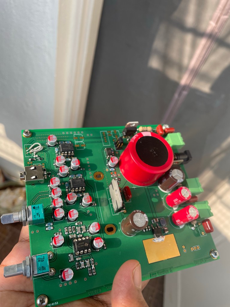
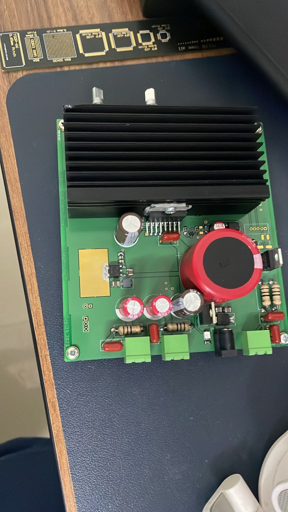
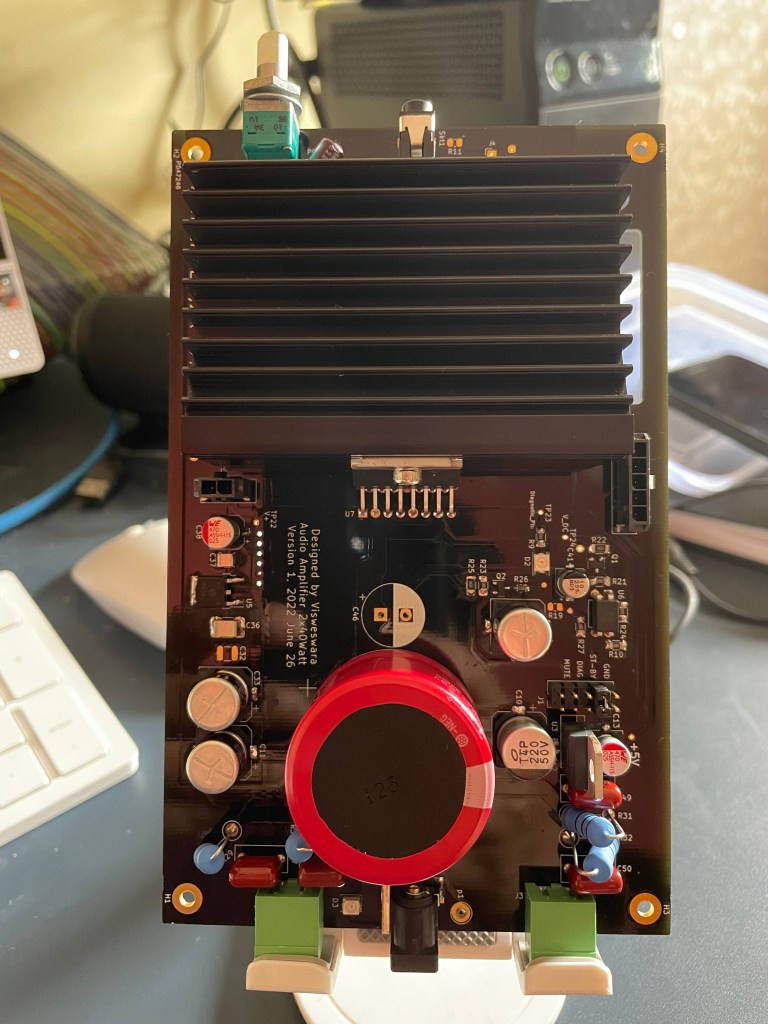
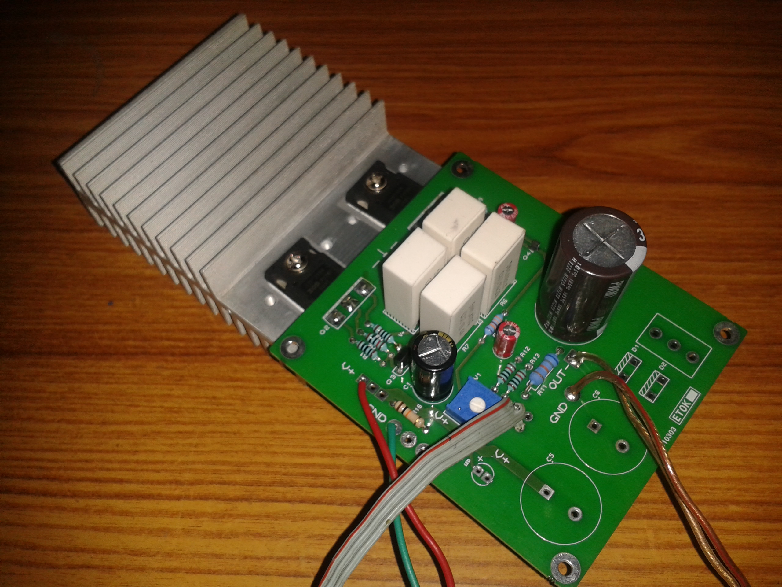
Prototype of amplifier:
.

Assembly instructions:
- Q3, Q4 and Q5 must be attached on the same heatsink, thermal insulators(mica) should be used for Q3 and Q5 to avoid short circuit of Power transistor Collector terminals of each, as center terminal is attached to main tab/body inside of transistor
- Adjust RV1 to 472 Ω
Specifications:
Output Impedance: 0.039 Ω
output : 12watts at 0.28% into 4 Ω driver(loud speaker)
Capable of driving loudspeakers of impedance range 2-16 Ω
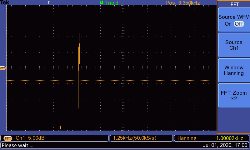 FFT response of the amplifier we see only fundamental and delivering 11watts RMS into 4.7E power resistor
Note: If you want STEREO for the other channel just duplicate the same, I have configured mine in mono channel by adding two 100E resistors at the input. Schematic posted here is a single channel.
Components:
Semiconductors:
- U1A, U1B and U1C OPA2134 (Texas Instruments)
- Q1 BD139 (ST microelectronics)
- Q2 BD140 (ST microelectronics)
- Q3, Q5 TIP3055G (ST microelectronics)
- Q4 ZTX450 (Diodes Incorporated)
Passive:
- R1 1K 1/4watt
- R3 , R5 330 1/2watt
- R4 100 1/4watt
- R6 , R7 0.22Ω, 2watt
- R8 , R9 47K 1/4watt
- R10 10Ω , 1watt
- R11 4.7K 1/4watt
- R12 82K 1/4watt
- R13 1.8K 1/4watt
- RV1 1K, trim potentiometer
- C1, C2 10uF, 50V electrolytic
- C3, C9 1uF 50V ceramic
- C4 4.7uF, 50V ceramic
- C5, C8 100nF 50V ceramic
- C6 220uF, 50V electrolytic
- C7 2200uF electrolytic
- C10 47pF 50V ceramic
Miscellaneous:
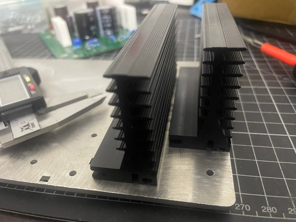
- Heatsink
- Thermal insulators or mica with screw fittings
- LS1 loudspeaker 4Ω, 20watt rated.
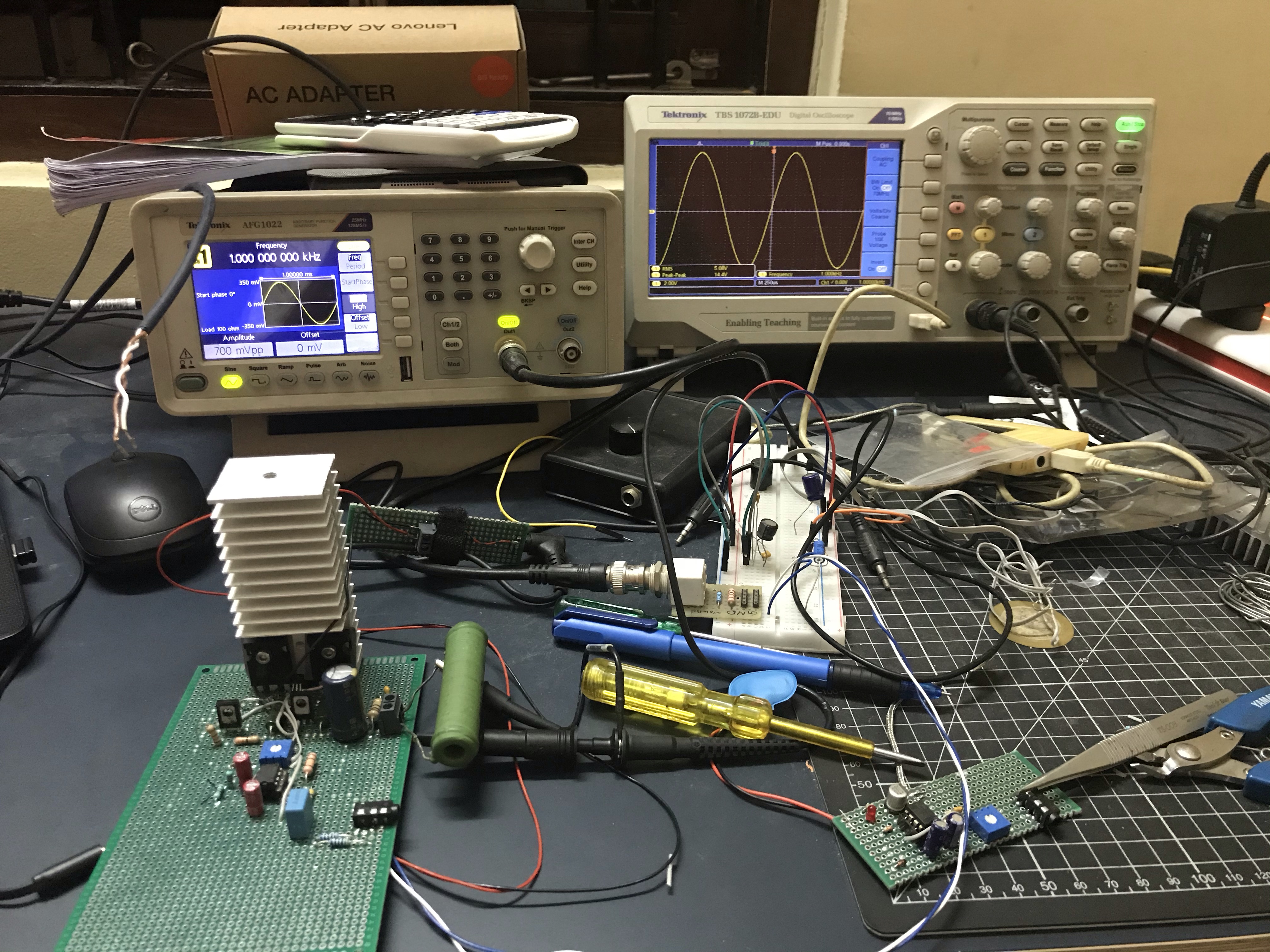
Equipment used to validate the amplifier circuit:
- Function generator AFG1022
- Scope TBS1072
- 20V, 3A adapter
- Fluke 115 DMM
- Power resistors 3.33 Ω 12watt and 4.7Ω 25watt
I will be very happy if you want to make this circuit. If you do, send me the pictures of your circuit, would like to see. If you feel any trouble in building this, let me know. Happy building.