I am always interested in building radio circuits. am transmitter, for construction, I used copper clad boards and really like the construction, not neat though, I do remember that I sprayed thicke…
Source: AM transmitter
I am always interested in building radio circuits. am transmitter, for construction, I used copper clad boards and really like the construction, not neat though, I do remember that I sprayed thicke…
Source: AM transmitter
article name: LME49710 audio amplifier
published on Electronics For You magazine june 2016 issue (south asian most popular magazine)
I am always interested in building radio circuits. am transmitter, for construction, I used copper clad boards and really like the construction, not neat though, I do remember that I sprayed thicker coats of lacquer on the board before laying the parts on it.
circuit diagram: 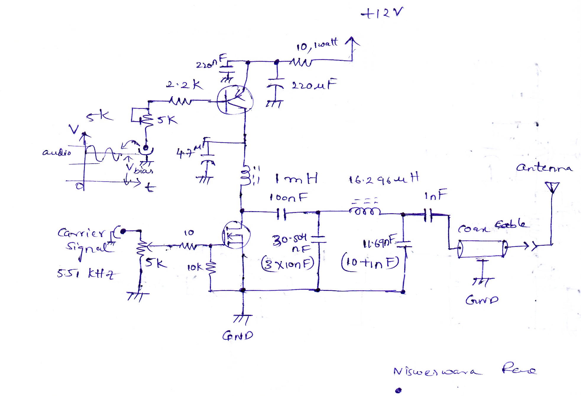

back panel


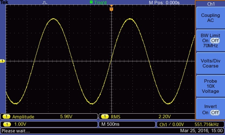
Carrier signal generator program:
it is simple just a PWM code, 16bit timer module in fast PWM
//FUSE bits
/*
BODLEVEL = DISABLED
RSTDISBL = [ ]
DWEN = [ ]
SPIEN = [X]
WDTON = [ ]
EESAVE = [ ]
BOOTSZ = 2048W_3800
BOOTRST = [ ]
CKDIV8 = [ ]
CKOUT = [ ]
SUT_CKSEL = EXTFSXTAL_16KCK_14CK_4MS1

EXTENDED = 0xFF (valid)
HIGH = 0xD9 (valid)
LOW = 0xE7 (valid)
*/
#define F_CPU 16000000UL
#include "avr/io.h"
#include "avr/interrupt.h"
#include "avr/sleep.h"
#include "util/delay.h"
void timer1(void);
void timer1()
{
        /*
         configure the timer1 module fast PWM mode
         Freq_OCR1A_PWM = F_CPU /(N(1+top)) = 16MHz/1(1+top)
         top = ICR1  */

    TCCR1A |= 1<<COM1A0 | 1<<WGM10 | 1<<WGM11;
    TCCR1B |= 1<<WGM12 | 1<<WGM13;
    TCCR1B |= 1<<CS10;
    ICR1 = 27.4;
}

int main(void)
{
    DDRD = 0x00;
    PORTD = 0x00;
    DDRC = 0x00;
    PORTC = 0x00;
    DDRB |= 1<<PINB1; // declaring PINB1 as output
    timer1();
    sei(); //enable interrupt
    while(1)
    {
        OCR1A = ICR1/2; //50% duty cycle
    }
}
we can also use schmitt trigger for this simple application, i used micrcontroller because i will include SWR meter in the future.


ah yes i know the circuit construction looks really bad, it is working 😀
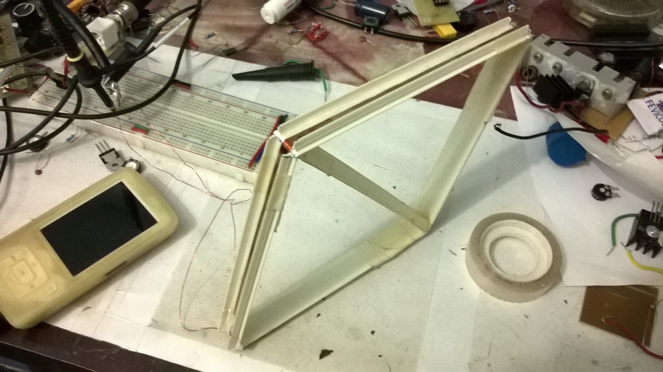
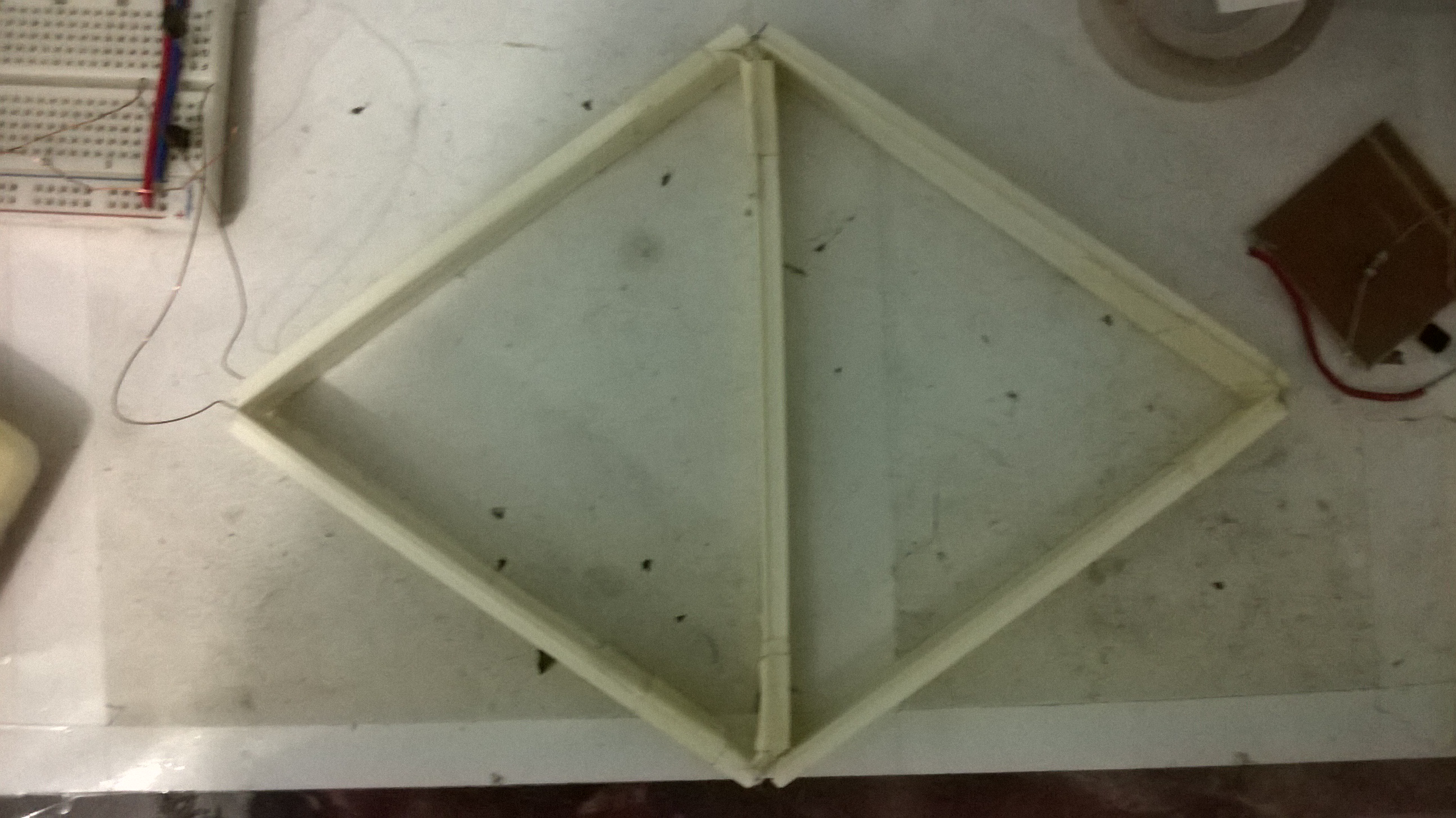
i used this Loop antenna and with low power works really good
Video
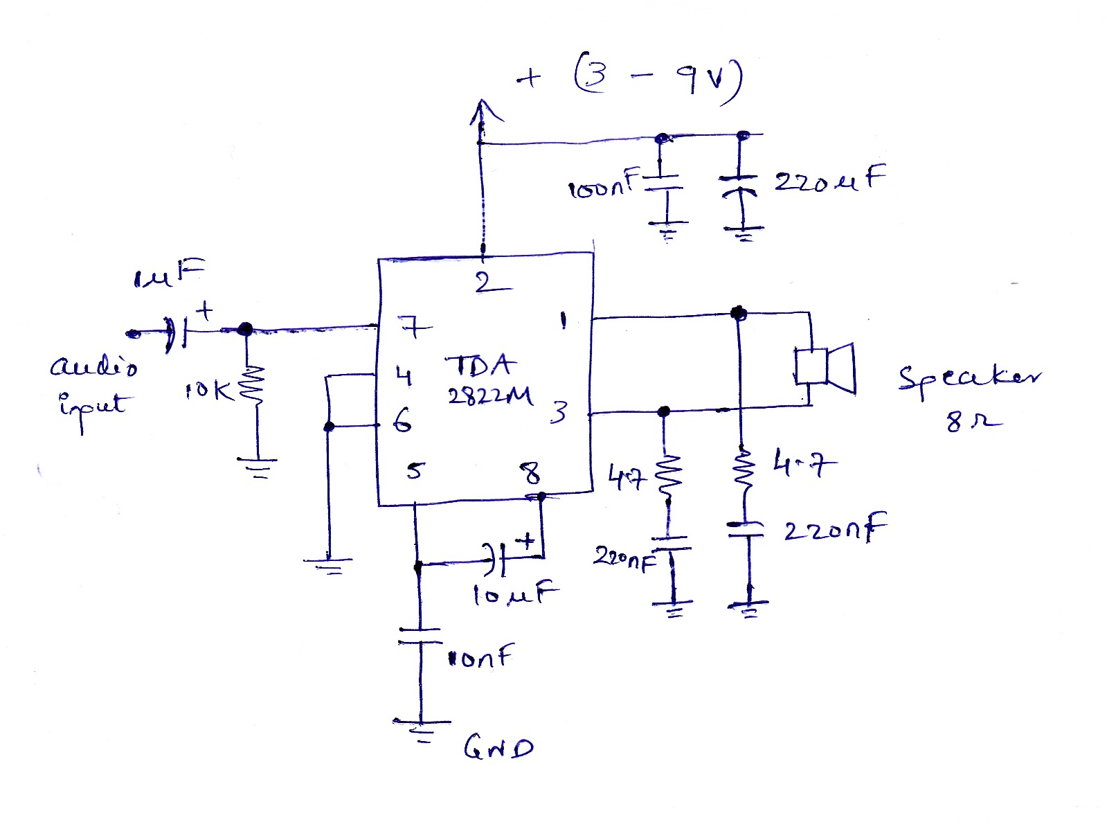
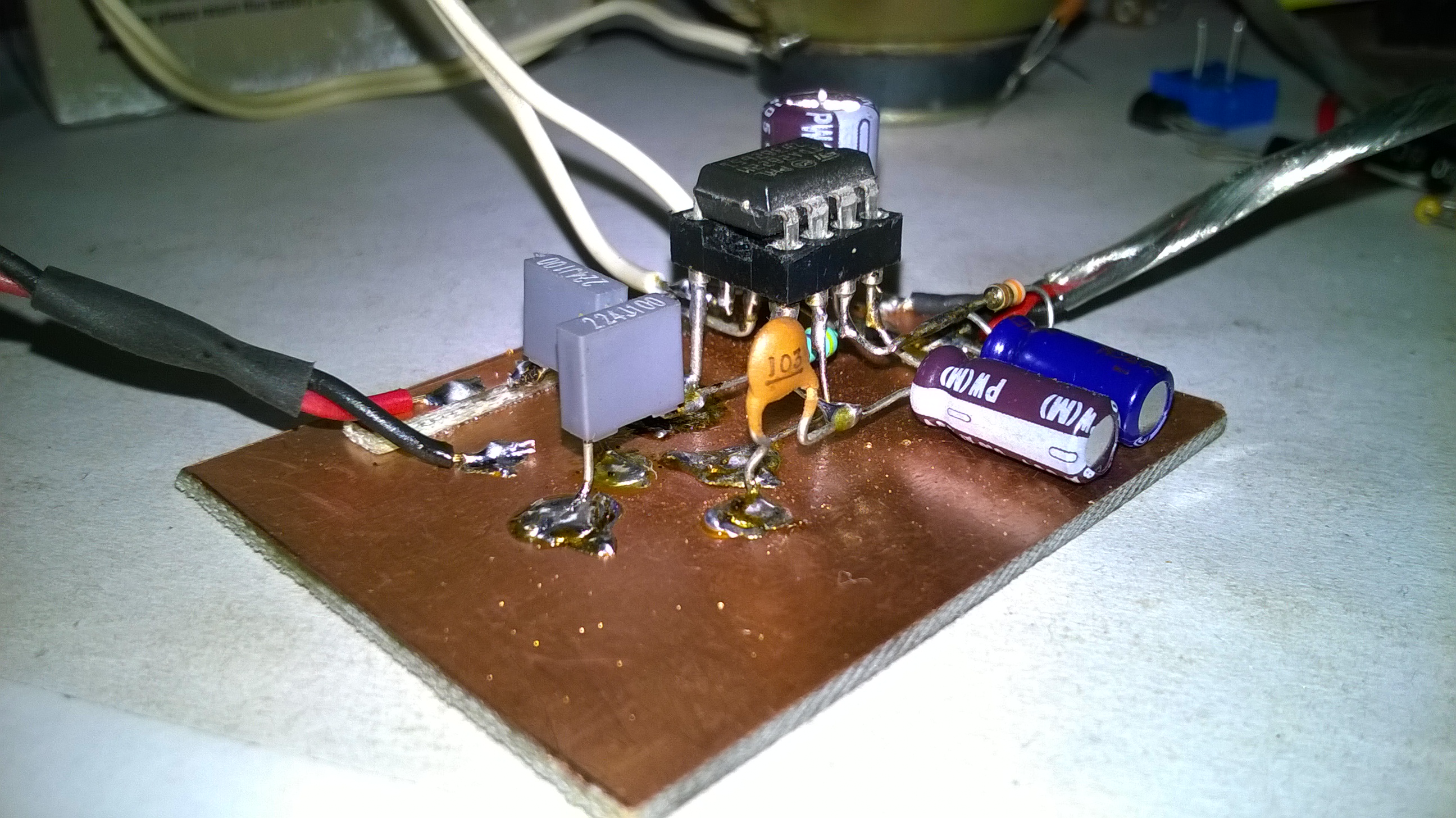
This is a part of my RF transceiver project, no parts for building tranceiver yet , so i have started with the audio amp circuit, amplifier circuit is based on TDA2822M chip which is configured in bridge mode and I used a single sided Copper plated board for Manhattan construction. 😛
circuit:
(nothing new it is from the datasheet)
my construction


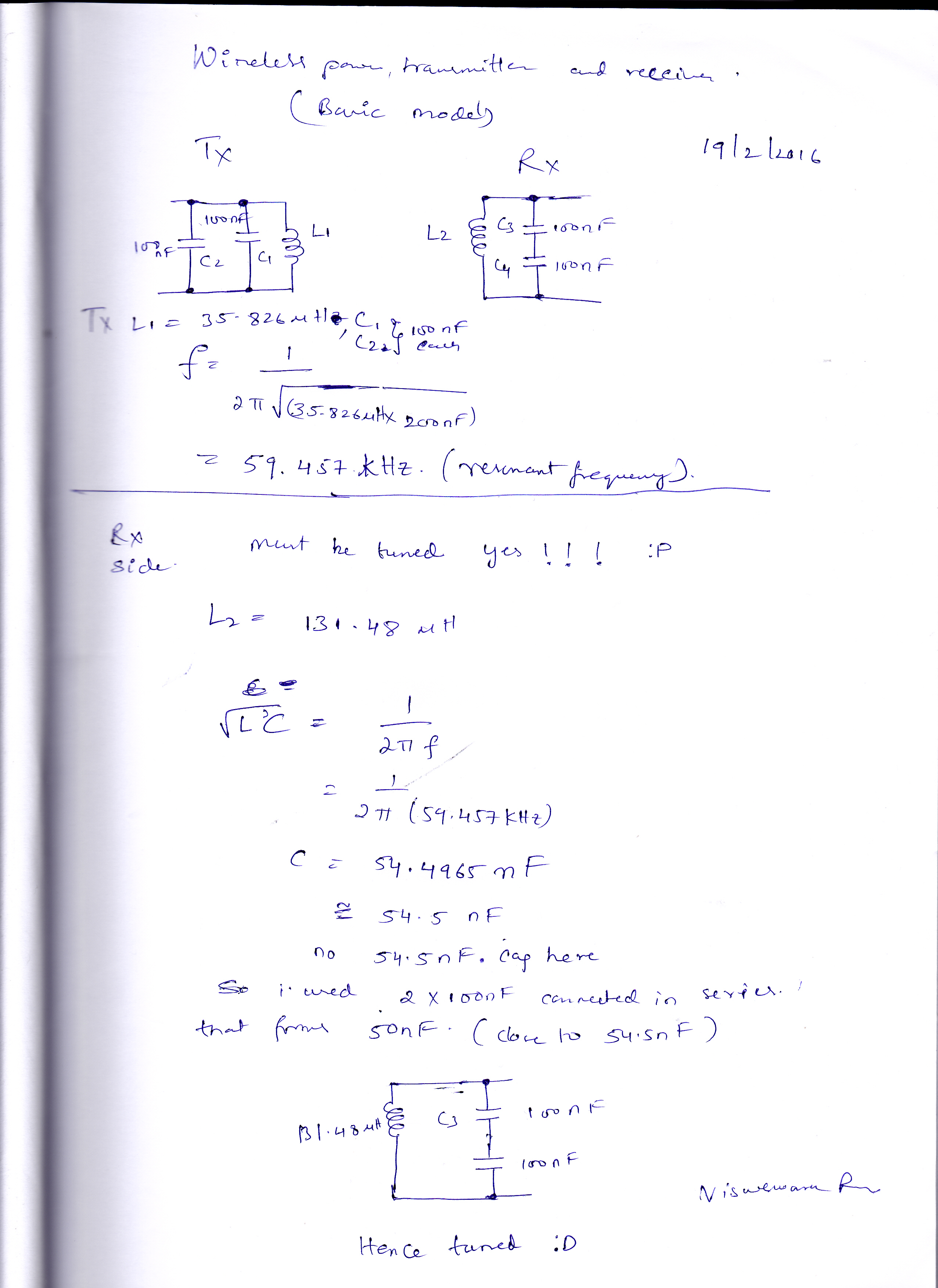
working model of wireless power transmitter and receiver. The Transmitter and Receiver coils with capacitors connected to each coils, forms a tank circuits that resonates with a frequency of f = 1/(2π√(LC)), if the two resonant circuits resonating at the same frequency and were brought to close, the energy transferred from transmitter to receiver…
so, the frequency of transmitter and receiver must be tuned for different inductance values of transmitting coil and the receiver coil…
L1 = 10turns , 160mm dia of 18SWG (transmitter coil) = 35.826uH
L2 = 20turns, 160mm dia of 18SWG(receiver coil) = 131.48uH
i have calculated the inductance of Tx and Rx coils using oscilloscope and the pulse generator.
paper work:
schematic:
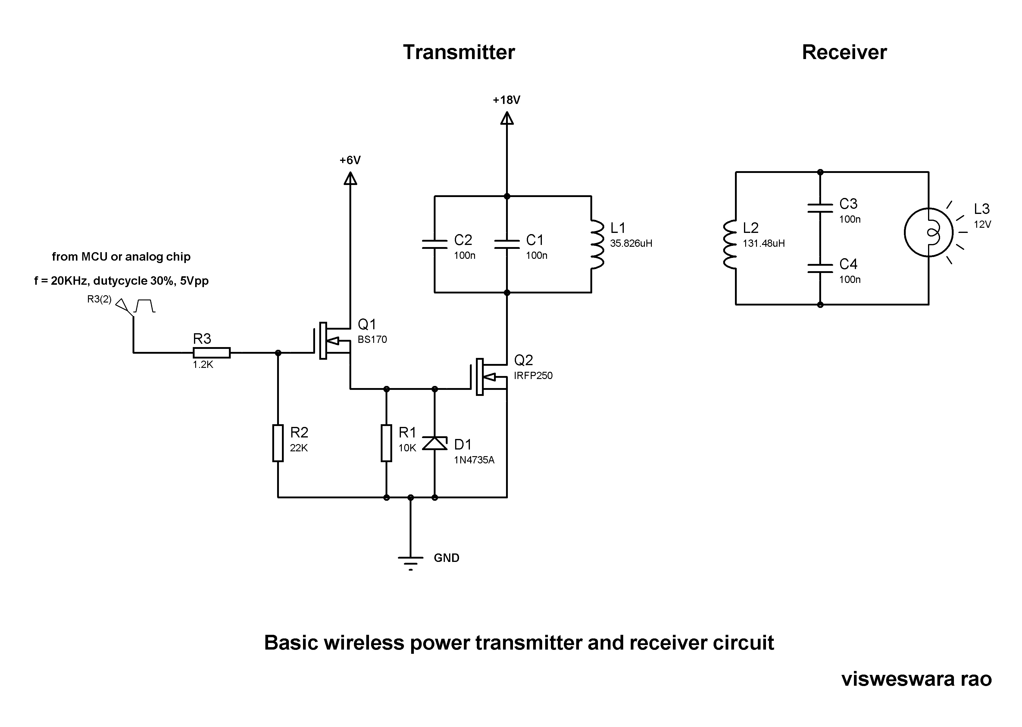
circuit is simple, apply a pulse of 20KHz, 30% duty cycle of 5Vpp use MCU or analog chip or opamps or schmitt trigger circuit.
BS170 is a lower power MOSFET serves as a gate driver for the power MOSFET IRFP250N, D1 (1N4735A) a 6.2V zener so the gate to source voltage (Vgs) is always less than 6.2V. L1 and C1 forms a tank circuit that resonates with a frequency of 59.457KHz. (transmitter )
resonating frequency of both transmitter and receiver must be same f1 = f2 = 59.457KHz
therefore 1/(2π√(L1C1) = 1/(2π√(L2C2)
(L1C1) = (L2C2)
therefore C2 = 54.4965nF
receiver must be detuned to the frequency using LC tank formed by L2 = 131.48uH therefore C2 = 54.4965nF (no 50nF, 1nF cap’s in my lab so i used 2 of 100nF capacitors connected in series that forms equivalent capacitance of 50nF which is little close to 54.5nF.
note: the capacitors must be type of polyster or polysulphide and atleast 200V rated..
here is my setup:


This is a LDR operated switch circuit, the LED’s ON when no light is present in the room.
circuit diagram and my construction pictures:

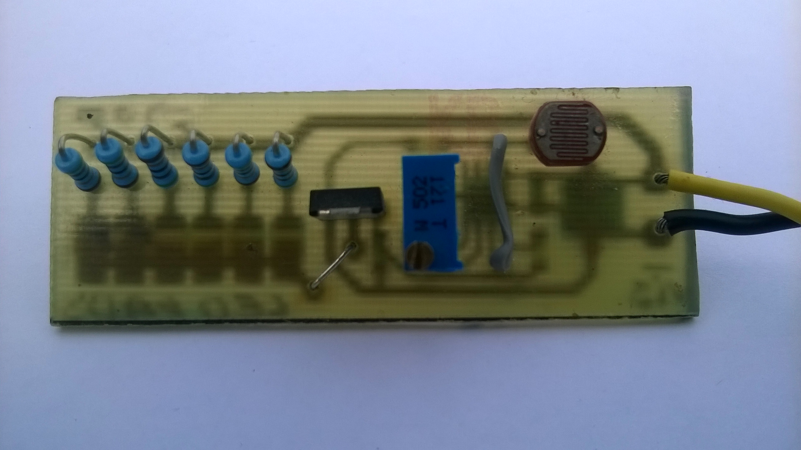
LDR (light dependent resistor) is a passive optical transducer, the resistance of LDR decreases with increase in light intensity, LDR or photoresistor is applied in light sensing detecting circuits, light or dark activated switches. The resistance of LDR is in the order of few MΩ in the dark and few hundreds of Ω in light….
working: RV1 (variable resistor) sets the reference voltage at the non-inverting pin(V+) of opamp(LM358). LDR and R1(10K) forms voltage divider network , the voltage at the inverting pin(V-) of opamp is low when the LDR in dark , the LDR resistance in the dark is around 10MΩ so the less the voltage drop across the R1(10K) therefore V- is LOW, the voltage at the non-inverting pin is very high which is also the reference voltage set by the trimmer potentiometer(RV1) .
so, Vout = (V+) – (V-) ( since V- << V+) therefore Vout =V+ , the Vout is high, the MOSFET comes into conduction,simply LEDs ON in the dark.. the drain current of the MOSFET set by the R2 and R3 resistors. since the MOSFET is voltage controlled the drain current is high the more the voltage drop across the R3 which is Vgs (gate to source voltage). the Vgs of the MOSFET must be greater than the threshold voltage(2.5V for NTD4963).
D1-D6 are the power LED’s , R4-R9 current limiting resistors, c1 and c2 are decoupling cap’s to remove noise.
This is the small audio amplifier circuit, with decent power output of 3watts RMS into 4ohms load.
as you can see the pictures of my construction:
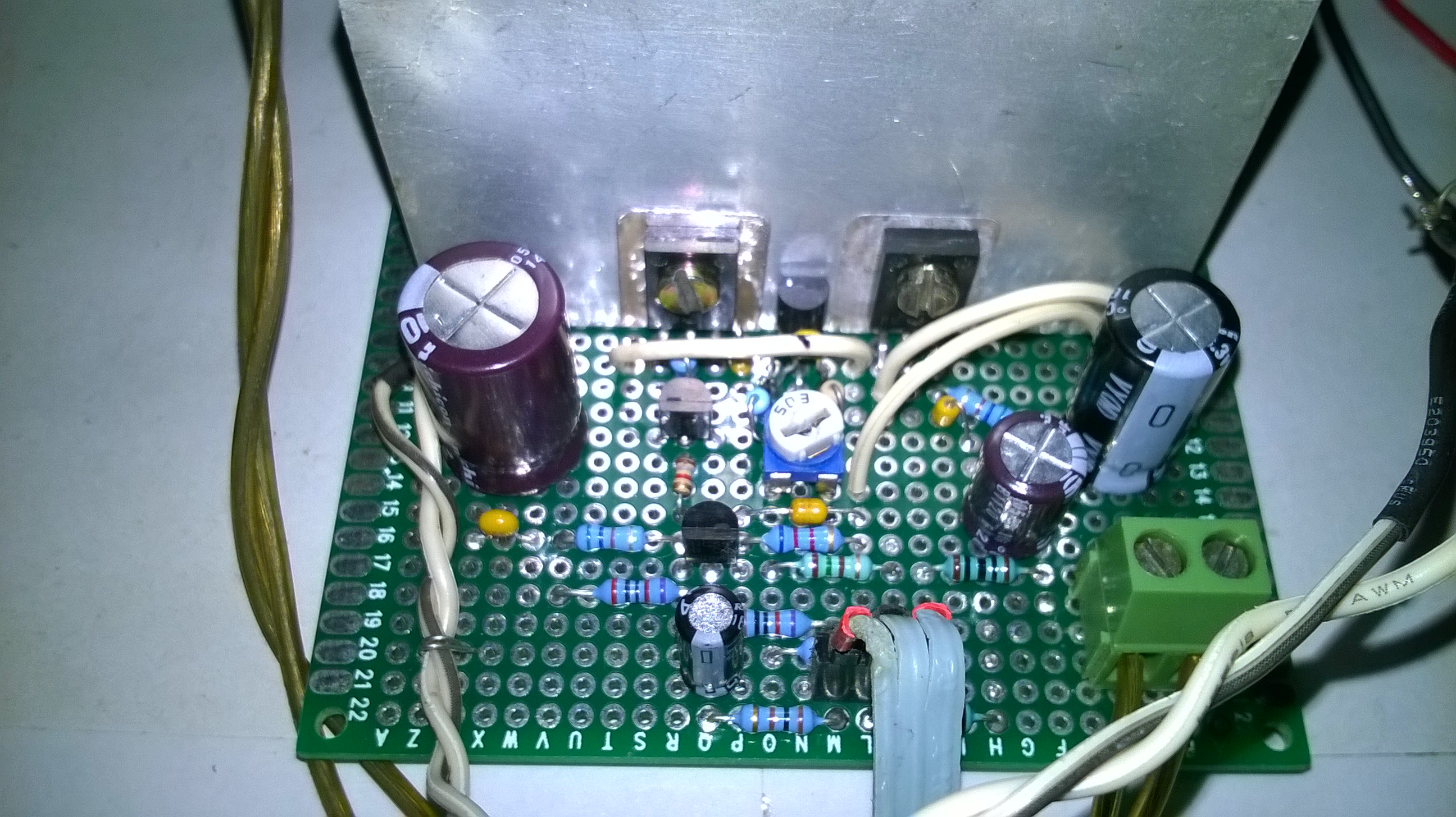


circuit diagram:
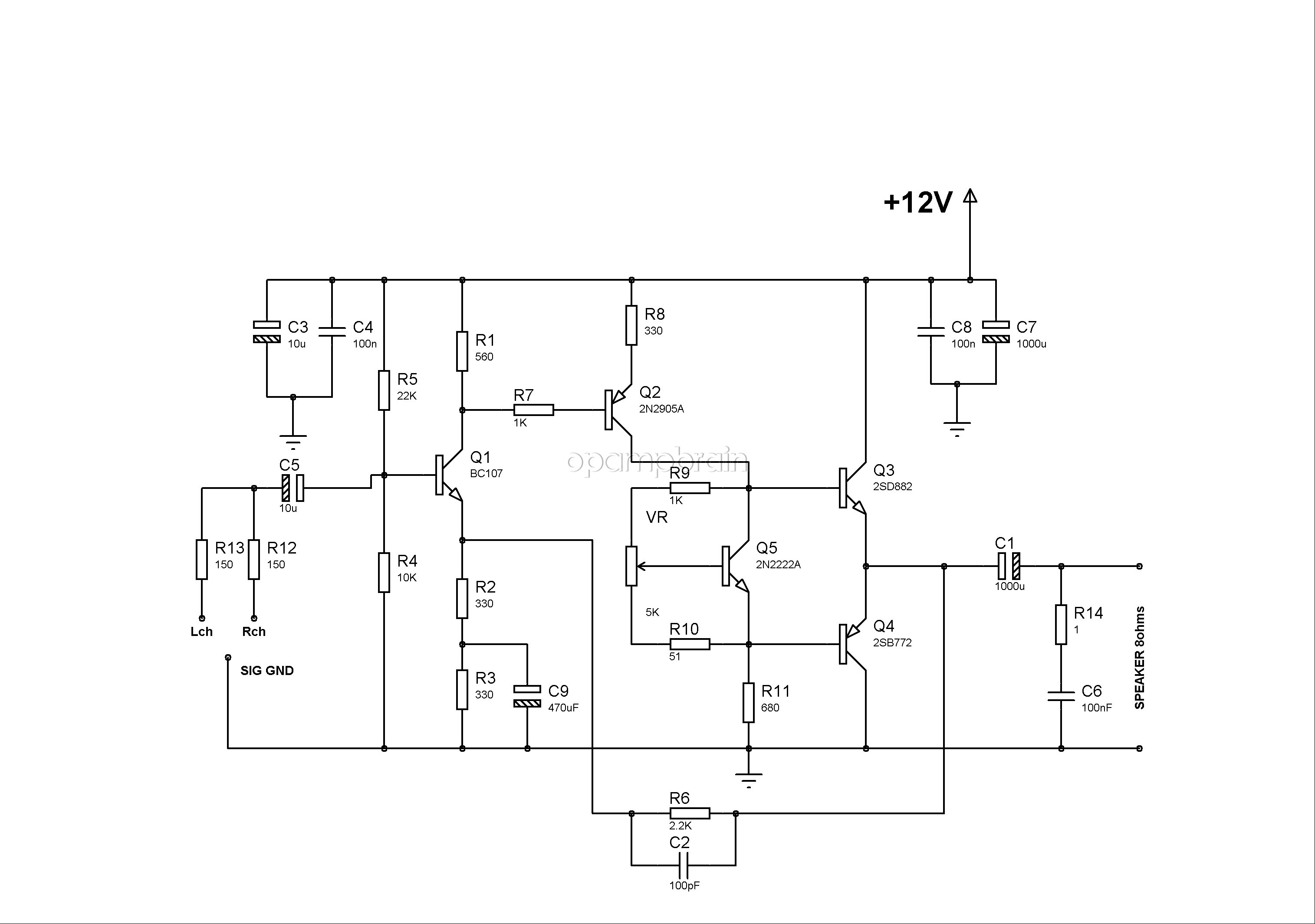
R4,R5 resistors forms voltage divider and biases the transistor Q1. the voltage across the R4 is (Vin*R4)/(R4+R5) 3.75Volts
R1 560 ohms set the collector current Ic of Q1 = (Vin-Vc)/560. Vc = 9.4volts measured with respect to GND so Ic = (12-9.4)/560 = 4.642mA
R2,R3 are the emitter resistors connected to Q1, since the Q1 is the input transistor of the amplifier circuit, so small ac signal appears across the emitter resistors, therefore low impedance path must be created to bypass the ac signal using capacitor C9 the value of c9 can be calculated by taking the two considerations into picture,
one is audio amplifier must cover the frequency range from 20Hz-20KHz and the other is the reactance of the capacitor should be 1/10 of the emitter resistance or less than the emitter resistance therefore Xc = 1/(2πfC) the c = 1/(2πfXc) , from this equation the capacitance is max at the lower frequency(20Hz) and Xc must be 1/10 of the emitter resistance
c = 1/(2 π×20×330/10) = 120.57uF = 120uF (which is standard) but rare 150uF is also standard also rare, I used 470uF.
Q2 , 2N2905A of motorola is the driver transistor(class A), this transistor is little old, you can use bd140 or 2N3906 instead, R7 is the base resistor and R7 is the collector resistor Q2 to keep the transistor in active region.(not a big gain at this stage)
R9,R10, VR 5K pot and Q5 , 2N2222A (can be 2N3904) forms the Vbe multiplier circuit to eliminate the cross over distortion, adjust VR to 1.7K up in series to the 1K(R9) s0 it forms (1.7K+1K). R11 and Vbe multiplier circuit controls the quiescent current to have thermal control over output the Q5 must be mounted to the main heatsink. this Vbe multiplier is a biasing diode but adjustable voltage drop.
Q3(CL100),Q4(CK100) are the output transistors. can also be replaced with famous bd139 and bd140. or 2sd882 and 2sb772
C1 is the output capacitor which is 1000uF, if you want to have good low frequency response , 3300uF is good.
R6, 2.2k (feedback resistor) in parallel with C2 1nF ceramic capacitor, creates a pole frequency of about 1/(2πRC) = 72.343KHz , feedback system keeps the amplifier linear and stable operation.
R14,C6 is to remove the high frequency noise..
C3,C4,C7,C8 are decoupling capacitors to remove high frequency, mid frequency and low frequency noise in the power supply lines
C5 is the input capacitor C5 and R4 together forms a high pass filter cutoff-frequency is 1/(2π×10uF×10K) = 1.59Hz.
R13,R12 (150 ohms) combines both the channels this resistors must be greater than 40 ohms, or else , effects the source device (ipod or music player etc…..)
here are the oscilloscope waveforms of neat 100KHz, square, ramp and sine wave ( R_load 7.5ohms )


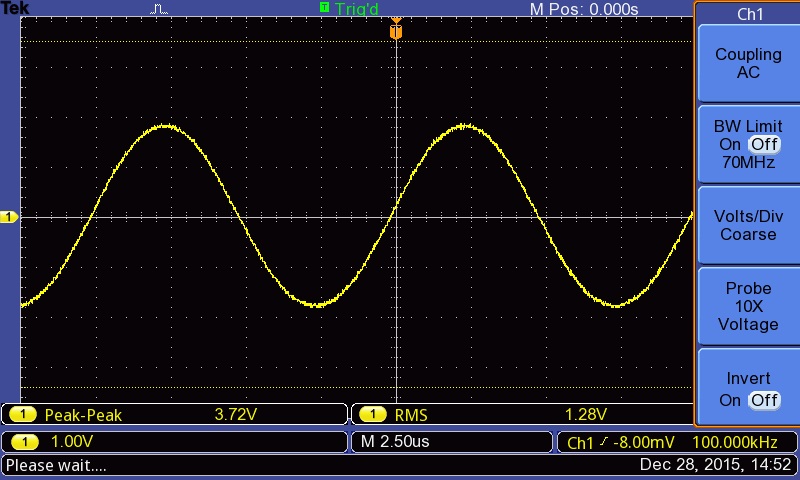
this amp sounds really good, from the scope results i did calculated THD, it is 2.5% at 3watts RMS output. frequency response is flat from 30Hz to 100KHz 😀
IR emitter:
It is a LED emits infrared light (940nm typically) applications of IR LED: like optical counters, free air data transmission, infrared remote control, card readers , etc….
photodiode (type of optical transducer)
photodiode is a high speed diode used to convert current to voltage, it is reverse biased with constant voltage.
Sensor module circuit diagram:
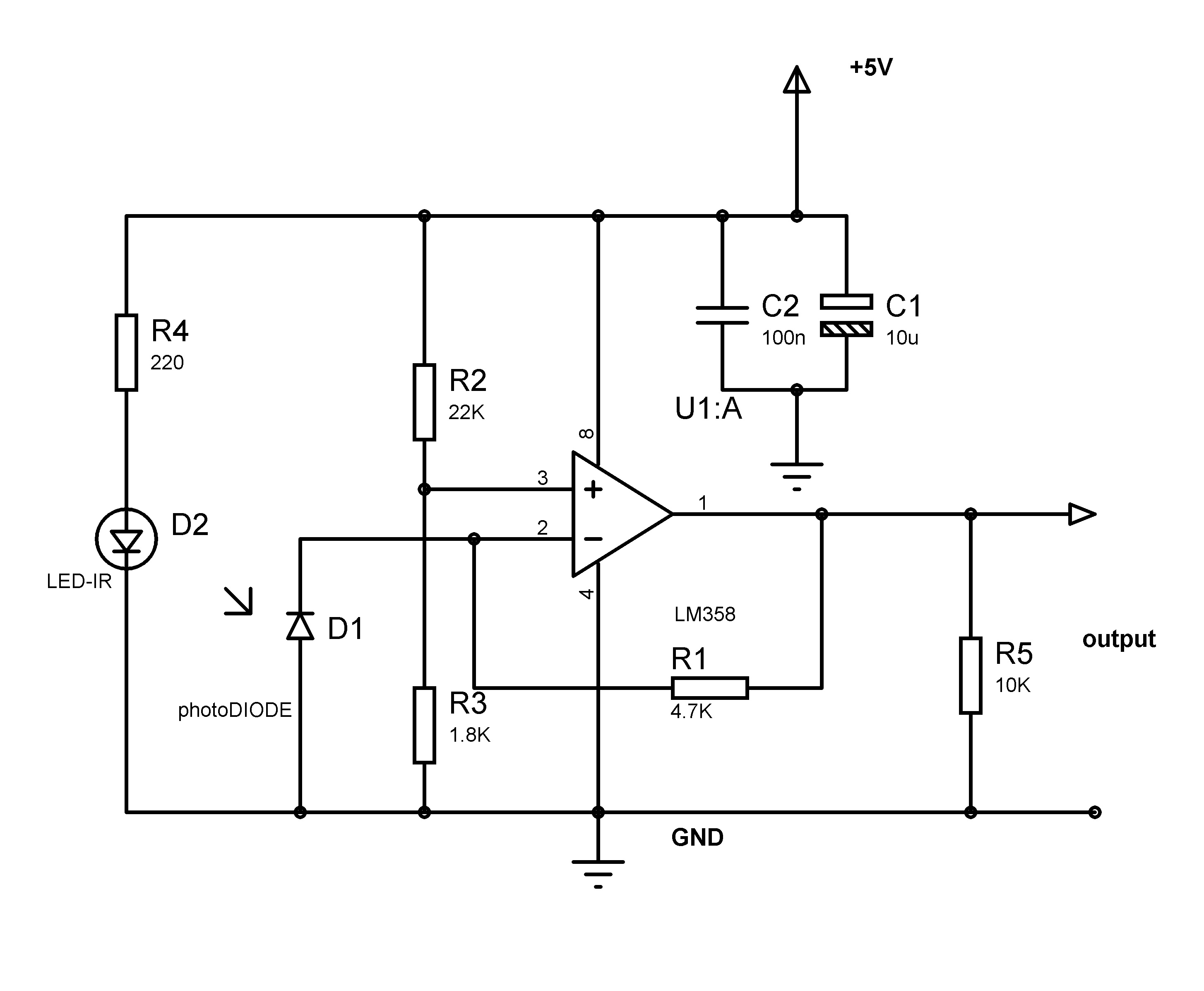
TCRT5000 sensor
opamp LM358
R2 and R3 for biasing the non-inverterting terminal of opamp(LM358), voltage at non-inverting terminal = Vin(1.8K)/(22K+1.8K) = 0.378V (378mV).. that is also the voltage at the pin1 of opamp with refered to ground(GND) when no IR light on photodiode. when full IR light on photodiode the Vout = 3.5V (which is max)
R1 sets the reverse bias voltage across D1(photodiode), in this condition the current flowing through the D1 is in the range of nA typically.
R4 sets the constant current that flows through the IR-LED D2
the forward voltage range is around 1.25 to 1.5V typically, the max current it can handle is 60mA so R4 = (Vin-1.25)/20mA = 187.5ohms if Vin = 5V (220ohms on board)
C2 and C1(decoupling caps) C1 electrolytic reduces the noise voltage created by the low frequency and mid frequency and C2 the low ESR ceramic cap reduces the high frequency noise in power supply lines
here is my construction, it looks ugly, ahh but working fine 😀

the output of sensor module connected to the scope, as you can see the voltage varies, the photodiode starts conduction when the IR light from the emitter is reflected on it, Vout is proportional to the current that flows through the photodiode.

